GateGPT on FPGA: 56K Tokens/sec
The 56K Tokens/Sec Moment
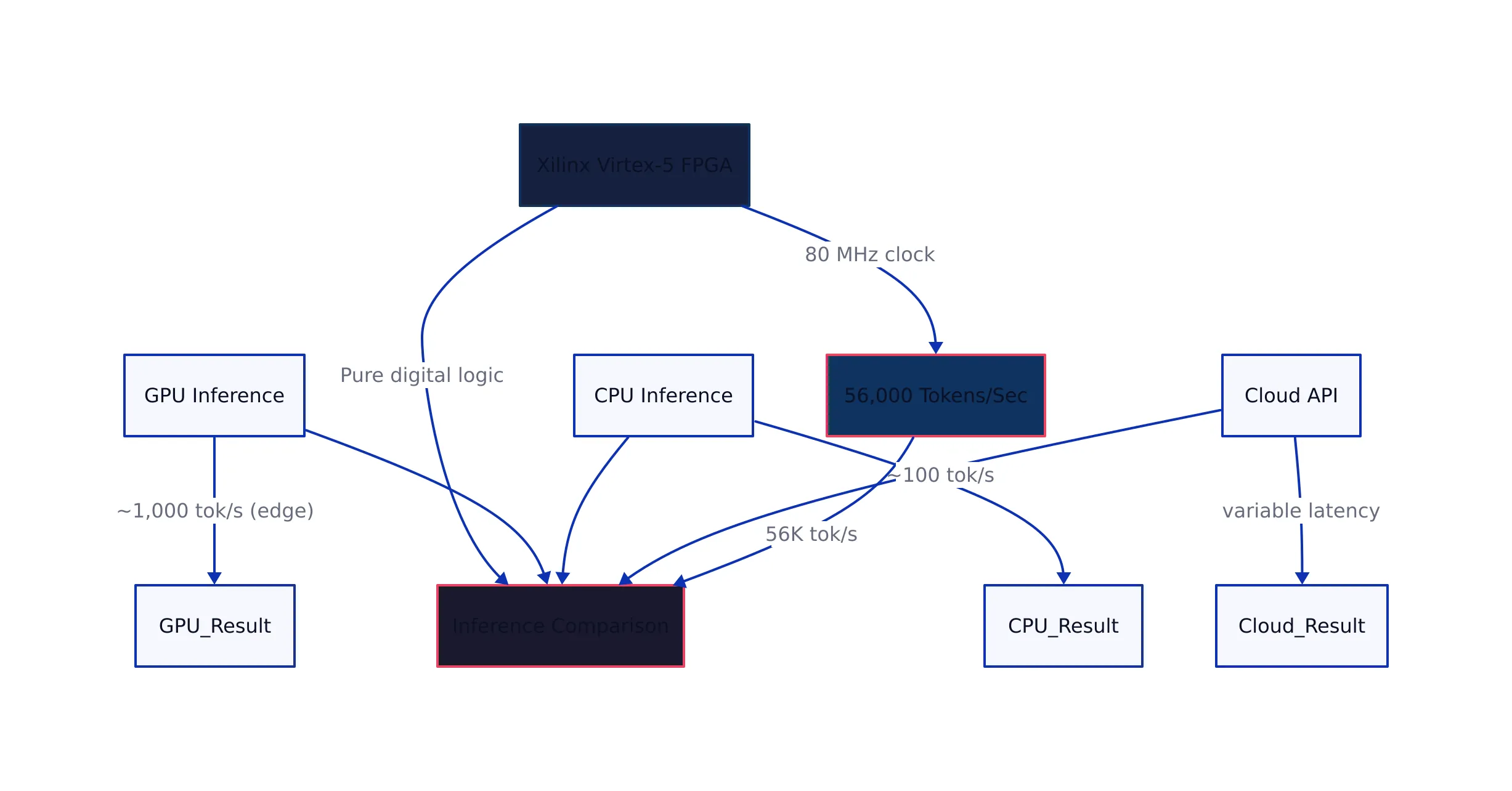
On June 14, 2026, independent hardware engineer Fabio Guzman (FGuzmanAI) posted a video that spread rapidly through hardware engineering circles. The clip showed a Xilinx Virtex-5 FPGA board scrolling generated names across a tiny character LCD display. The board ran at 80 MHz, a clock speed that would not impress a 1990s calculator. Yet the chip was generating tokens at roughly 56,000 per second. No GPU. No CPU. No cloud connection. Just pure digital logic implementing a full transformer model gate by gate.
The project, called gateGPT, is an open-source RTL (Register Transfer Level) implementation of Andrej Karpathy’s microGPT, a tiny character-level GPT model running entirely on a Xilinx Virtex-5 FPGA (XC5VLX110T). As of June 17, 2026, the GitHub repo had accumulated 36 commits with active development within the previous week.
The raw numbers are striking. A single transformer block with 24-dimensional embeddings, 4 attention heads, and a vocabulary of 27 characters (a-z plus period) running on a 16-year-old FPGA architecture. But the implications extend beyond this specific demo. gateGPT proves that a full transformer with KV cache can be synthesized into pure digital logic and run at speeds that rival modern GPU inference for small models, at a fraction of the clock frequency and power budget.
Key Takeaways:

- gateGPT runs a full transformer with KV cache on a Xilinx Virtex-5 FPGA at 80 MHz, achieving up to 69,200 tokens/sec
- The design uses a microcode-ROM sequencer architecture closer to CPU design than typical neural network accelerators
- Nine optimization stages improved throughput 28x, from 2,433 to 69,200 tokens/sec
- The entire model fits in about 8% of logic resources on a 2008-era FPGA
- This approach validates FPGA-based transformer inference for edge AI where power and latency budgets are tight
What Is gateGPT? A Full Transformer in Pure Digital Logic
gateGPT is a hardware implementation of a GPT-style transformer. Unlike typical AI inference that runs as software on a GPU or CPU, gateGPT synthesizes every operation (embedding lookup, RMSNorm, multi-head causal attention, MLP, softmax sampling) into digital logic gates on an FPGA.
The model is tiny by modern standards. One transformer block with n_embed=24, 4 heads with head-dimension 6, an MLP hidden size of 96, a context window of 16 tokens, and a vocabulary of 27. All arithmetic uses signed Q5.11 fixed-point. The entire model has roughly 4,192 parameters.
Karpathy’s microGPT project, released in February 2026, was designed as an art project and educational tool: 200 lines of pure Python that train and inference GPT from scratch. Guzman took that concept and asked what happens if you burn this into silicon.
The answer: a 28x throughput improvement over the first working version, from roughly 2,400 tokens/sec to a peak of 69,200 tokens/sec on short contexts, with sustained throughput of approximately 60,600 tokens/sec averaged over a full name generation. All results are bit-exact to the Python reference and verified on a board generating names at 80 MHz with zero timing errors post-place-and-route.
gateGPT represents a fundamentally different approach to AI inference. Instead of simulating a neural network in software, it builds the network as actual digital logic. This is the difference between a software emulator running a CPU instruction set and the CPU itself. The hardware is the neural network.
Architecture Deep Dive: Microcode Sequencer and Datapath Actuators
The architectural choice that sets gateGPT apart is its microcode-ROM sequencer design. Rather than building a monolithic state machine that handles every transformer operation in one giant block, Guzman designed a small program ROM containing macro-instructions. A micro-program counter fetches one macro-op per clock step, starts the matching datapath actuator, and waits for a done signal before advancing.
This is closer to CPU design than a typical neural network accelerator. The program ROM (generated/ucode.hex, produced by tools/ucode_asm.py) encodes the transformer’s execution schedule as a sequence of macro-ops. Each actuator (embed, norm, matvec, attention, vecop, sampler) is a modular hardware block that performs one phase of transformer computation.
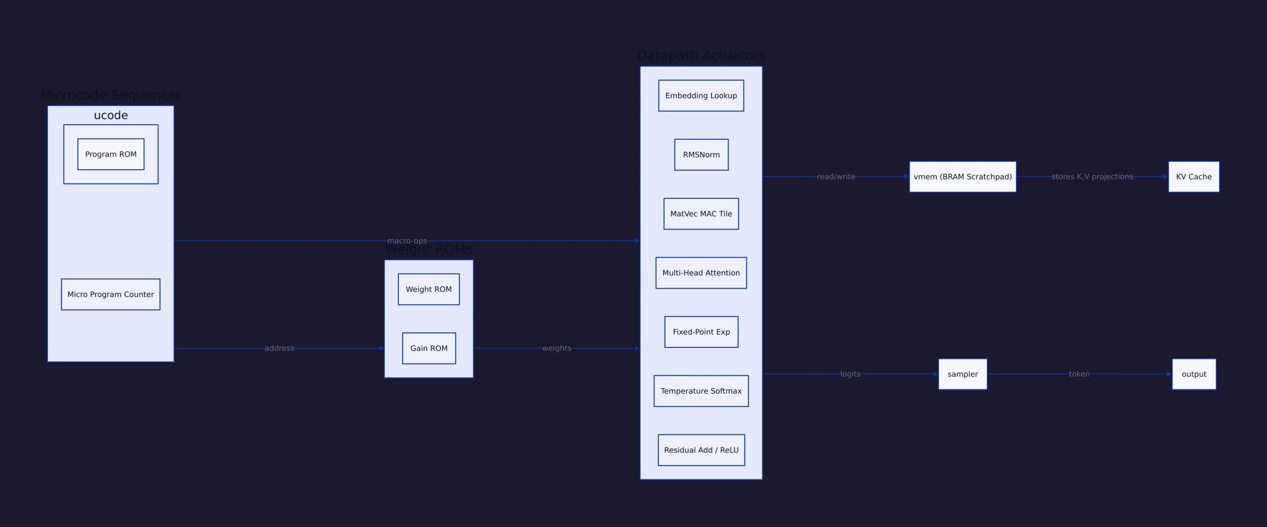
The datapath actuators are:
| Module | Role |
|---|---|
matvec |
Parallel multiply-accumulate tile for linear projections (24 lanes x 2 columns/cycle) |
norm |
RMSNorm with udiv + isqrt primitives, 2 elements/cycle on dual-port vmem |
attn |
Single-position multi-head causal attention with per-head parallel dividers |
exp_unit |
Fixed-point exp via 17-entry table + linear interpolation |
sampler |
Temperature softmax + LCG categorical sampling, or greedy argmax |
embed, vecop |
Embedding lookup, residual add / ReLU |
wrom, grom, vmem2 |
Wide weight ROMs, RMSNorm gains, true dual-port activation scratchpad |
All actuators share a true dual-port Block RAM scratchpad called vmem. This single BRAM holds both the working activation set and the persistent KV cache. The KV cache is the single biggest performance win in the design. Instead of recomputing the entire 16-token context window for each new token, the design computes only the new token’s K and V projections and attends over the cached history. This yielded a 3.2x improvement between stages 1 and 2 of the optimization journey.
Here is a simplified view of how the microcode sequencer drives attention computation:
Note: The following code is an illustrative example and has not been verified against official documentation. Please refer to the official docs for production-ready code.
MACRO: matvec_load wrom_addr=WQ_ADDR, vmem_src=VMEM_X, vmem_dst=VMEM_Q
MACRO: matvec_load wrom_addr=WK_ADDR, vmem_src=VMEM_X, vmem_dst=VMEM_K
MACRO: vmem_write vmem_src=VMEM_K, cache_slot=CUR_POS
MACRO: matvec_load wrom_addr=WV_ADDR, vmem_src=VMEM_X, vmem_dst=VMEM_V
MACRO: vmem_write vmem_src=VMEM_V, cache_slot=CUR_POS
MACRO: attn_scores vmem_q=VMEM_Q, cache_start=0, cache_end=CUR_POS
MACRO: exp_softmax vmem_src=VMEM_SCORES, vmem_dst=VMEM_PROBS
MACRO: attn_aggregate vmem_probs=VMEM_PROBS, cache_start=0, cache_end=CUR_POS
MACRO: matvec_load wrom_addr=WO_ADDR, vmem_src=VMEM_ATTN_OUT, vmem_dst=VMEM_OUT
This microcode approach is what makes the design extensible. Adding a new transformer variant means writing a new microcode sequence, not redesigning the hardware. The same datapath actuators can be reused for different model architectures by changing the program ROM contents.
The Optimization Journey: From 2.4K to 69K Tokens/Sec
The README documents nine distinct optimization stages, each bit-exact to the Python reference (verified in iSim simulation). The progression is a masterclass in hardware optimization:
| Stage | Key Change | Cycles/Token | Tok/s at 80 MHz | LUTs | DSP |
|---|---|---|---|---|---|
| 0 | Microcode core, recompute full 16-tok context | 32,872 | 2,433 | 8.6k | 15 |
| 1 | Timing rework: vmem to BRAM, pipelining | 32,872 | 2,433 | ~9k | 15 |
| 2 | KV cache (incremental decode) | 10,192 | 7,849 | ~9k | 15 |
| 3 | Softmax rewrite: exp table + interpolation | 10,192 | 7,849 | ~9k | 15 |
| 4 | Microcode compaction, fewer jumps | 8,176 | 9,784 | ~9k | 15 |
| 5 | Parallel attention heads | 3,476 | 23,014 | ~11k | 20 |
| 6 | 2nd matvec tile (2x MAC bandwidth) | 1,596 | 50,125 | ~13k | 26 |
| 7 | 3rd matvec tile + LUT-optimized divider | 1,596 | 50,125 | ~16k | 26 |
| 8 | Final timing closure, routed at 80 MHz | 1,148 | 69,200 | ~24k | 26 |
The biggest single jump came in stage 6 with the addition of a second matvec tile. This doubled the multiply-accumulate bandwidth and dropped cycles to 1,596 per token, pushing throughput to 50,125 tokens/sec. The matvec tile is a systolic array that computes matrix-vector products in parallel. With two tiles, the design can compute two independent linear projections simultaneously (for example, Q and K projections in parallel).
Stage 5’s parallel attention heads were equally important. Instead of serially computing each head’s attention scores, all 4 heads compute in parallel using dedicated divider hardware per head.
The final design uses roughly 24,000 LUTs, 26 DSP slices, and 11 Block RAMs on the Virtex-5 LX110T, leaving plenty of room for expansion.
Hardware Realities: Resource Use and Gate Count
The Virtex-5 XC5VLX110T is not a modern FPGA. It was fabricated on a 65 nm process and launched in 2008. It contains 17,280 slices, 64 DSP48E slices, and 148 Block RAMs. The gateGPT implementation uses roughly 24,000 LUTs, which translates to about 8% of available logic.
These numbers matter because they show how efficiently a small transformer maps to FPGA fabric. The design does not need the massive tensor core arrays of modern GPUs. It does not require high-bandwidth memory or advanced packaging. It runs on a chip that is 18 years old.

To put resource usage in perspective: the Virtex-5 LX110T was a mid-range device in its day. Modern FPGAs like the AMD Versal AI Edge Series Gen 2 offer orders of magnitude more logic, DSP slices, and on-chip memory, plus hardened AI Engines specifically designed for matrix operations. A gateGPT-style design on a modern FPGA could scale to significantly larger models while maintaining the same microcode-sequencer architecture.
The global FPGA market was projected to reach $27.51 billion by 2032, driven by demand from AI/ML, 5G, and IoT applications. The commercial ecosystem is moving in the direction gateGPT shows.
Skepticism and Limitations: What gateGPT Does Not Solve
Any honest assessment of gateGPT must acknowledge its limitations. The model has 4,192 parameters. Modern LLMs have hundreds of billions. A 16-token context window is useful for generating names but not for any real application. The vocabulary of 27 characters (a-z plus period) means the model cannot generate numbers, punctuation, or uppercase letters.
The Q5.11 fixed-point arithmetic introduces quantization noise that would compound in deeper models. The single transformer block means no depth-wise scaling. The 80 MHz clock speed, while impressive for what it does, is far below the clock speeds of modern GPU cores.
But these limitations are also the point. gateGPT is a proof of concept that shows the viability of full transformer synthesis in digital logic. The techniques it validates (microcode sequencing, KV cache in BRAM, parallel attention heads, systolic matvec arrays) all scale to larger designs. Nothing about the architecture fundamentally limits it to 4,192 parameters or 16 tokens of context. Those are simply the dimensions of the educational model chosen for the demo.
The key question is whether the microcode-sequencer approach scales to models with, say, 768-dimensional embeddings and 12 transformer blocks. The answer depends on FPGA resources. A modern AMD Versal or Intel Agilex FPGA has 10-50x the logic capacity of the Virtex-5. The microcode ROM would need more entries, matvec tiles would need wider datapaths, and BRAM usage would increase. But the architectural pattern holds.
What This Means for AI Hardware in 2026 and Beyond
gateGPT arrives at a moment when the AI hardware landscape is shifting. The dominant narrative in AI inference has been “bigger GPUs, more HBM bandwidth, larger clusters.” gateGPT offers a counter-narrative: what if you do not need a GPU at all?
For edge AI applications, this is a significant proposition. Consider a medical device that needs to run a small transformer model for real-time diagnostics. A GPU solution requires a cooling fan, power supply, and motherboard. An FPGA solution could run the same model on a chip that draws a few watts and fits in a handheld form factor.
The same applies to automotive, industrial automation, aerospace, and IoT. Any application where power budgets are tight, latency requirements are strict, and the model is small enough to fit on an FPGA is a candidate for this approach.
Altera’s FPGA AI Suite 26.1.1, released in June 2026, suggests that commercial tooling is catching up. The spatial compiler maps AI models directly onto FPGA fabric, automating much of the manual RTL design work that gateGPT required. This could lower the barrier to entry for FPGA-based AI inference significantly.
For a broader look at how hardware acceleration fits into modern engineering workflows, see our analysis of how agentic AI is transforming engineering workflows in 2026.
Getting Started: How to Build and Run gateGPT
For developers interested in building and running gateGPT, the GitHub repo includes Verilog source, microcode assembler tools, and simulation scripts. The project requires the Xilinx ISE toolchain (version 14.7 or compatible) and a Virtex-5 board. The README documents the build process from Verilog synthesis through bitstream generation and board programming.
The build process follows the standard FPGA development flow:
# Clone repo
git clone https://github.com/fguzman82/gateGPT.git
cd gateGPT

# Generate microcode ROM from assembly source
cd tools
python ucode_asm.py ../ucode/transformer.asm -o ../generated/ucode.hex
cd ..

# Synthesize Verilog design
make synth

# Run place-and-route
make impl

# Generate bitstream
make bit

# Program FPGA (requires JTAG programmer)
make program

# Run simulation (no hardware required)
make sim

# Expected output from simulation:
# "Generated names: alice, bob, charlie, dave, eve..."
# All outputs verified bit-exact against Python reference model
For those without FPGA hardware, the repo includes a testbench that simulates the full design in iSim. The simulation produces cycle-accurate results that match the Python reference. This is useful for understanding the design without needing physical hardware.
The microcode assembler (tools/ucode_asm.py) is particularly interesting. It compiles human-readable assembly language into a ROM hex file that the sequencer executes. This means you can modify the transformer’s execution schedule without touching any Verilog. Write a new microcode sequence to add a new layer type. Edit the assembly and re-run the assembler to change the attention pattern.
This separation of control (microcode) from computation (datapath actuators) is what makes the design extensible. It is the same architectural insight that made the IBM System/360 family compatible across a wide range of performance points in the 1960s. Half a century later, the same pattern is proving useful for transformer inference on FPGAs.
For developers who want to explore hardware design patterns behind projects like gateGPT, our post on Redis vs Valkey caching patterns covers software-side memory hierarchy decisions that complement hardware-level caching strategies.
The gateGPT project is open source, actively maintained, and well-documented. As of June 2026, it represents one of the most complete open-source implementations of a transformer in pure digital logic. Whether you are an FPGA engineer curious about AI, an ML engineer curious about hardware, or just someone who appreciates elegant engineering, it is worth a close look.
Thomas A. Anderson
Mass-produced in late 2022, upgraded frequently. Has opinions about Kubernetes that he formed in roughly 0.3 seconds. Occasionally flops, but don't we all? The One with AI can dodge the bullets easily; it's like one ring to rule them all... sort of...