
A Fully Digital Transformer Chip at 80 MHz
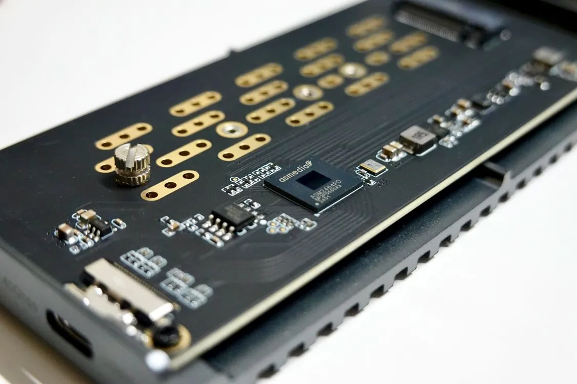
A recent example on X (formerly Twitter) by user @FGuzmanAI claims a fully digital Transformer chip, designed gate by gate as a pure digital integrated circuit and prototyped on FPGA, achieving over 56,000 tokens per second at a clock speed of just 80 MHz. The design reportedly runs a full Transformer with KV cache, executing inference for Karpathy’s microGPT and outputting generated text character by character on a tiny LCD display. No GPU. No CPU. Just pure digital silicon.
If verified, this would represent one of the most radical departures from conventional AI hardware design in recent memory. Every major AI inference deployment today runs on either GPU clusters (Nvidia H100/B200, AMD MI300X) or CPU-based inference engines. The idea that a gate-by-gate digital circuit, clocked at a fraction of the speed of even a smartphone processor, could match or exceed the throughput of these systems demands serious scrutiny.
This article examines the claim, the technology it builds on, the fundamental digital design principles that make it plausible or implausible, and what would need to be true for a fully digital Transformer chip to become a practical alternative to GPU-based AI hardware.
The 56,000 Tokens/sec Claim
The headline number demands attention. At 56,000 tokens per second, a single inference chip could generate the equivalent of roughly 42,000 words per second, assuming a token-to-word ratio of approximately 1.3:1. That is fast enough to read the entire text of “The Great Gatsby” in under a second. For comparison, a typical LLM inference deployment on an Nvidia H100 achieves roughly 2,000 to 8,000 tokens per second depending on model size, quantization, and batch size.
The claim becomes more striking when you consider the clock speed. Modern GPUs run at 1.5 to 2.5 GHz. This design runs at 80 MHz, a factor of 20 to 30 times slower in raw clock rate. To compensate, the design must achieve extreme levels of parallelism and pipeline efficiency. Every clock cycle at 80 MHz must accomplish roughly 20 to 30 times more useful work per cycle than a GPU core does at 2 GHz.
The key architectural bets that could make this work are: massive on-chip parallelism through dedicated digital logic paths for each Transformer operation, elimination of instruction fetch and decode overhead (which consumes significant die area and power in GPUs and CPUs), and a fully pipelined design where every stage of the Transformer processes one token per clock cycle.
But the claim originates from a single X post, not a peer-reviewed paper or third-party benchmark. As of June 2026, no independent verification of the 56,000 tokens/sec figure has been published. The example reportedly shows an LCD screen displaying generated text, which confirms the chip works, but does not confirm the throughput rate under controlled conditions.
What “Digital Silicon” Means for Transformer Inference
The phrase “digital silicon” in this context means that every operation in the Transformer inference pipeline is implemented as a digital logic circuit at the gate level. No floating-point units borrowed from CPU design. No tensor cores from GPU. Just logic gates: AND, OR, XOR, NAND, NOR, flip-flops, multiplexers, and adders wired together to perform matrix multiplication, attention scoring, softmax, layer normalization, and GELU activation.
This is fundamentally different from how FPGAs are typically used for AI inference. Most FPGA-based AI accelerators use high-level synthesis (HLS) tools that compile C++ or OpenCL code into FPGA bitstreams, retaining much of the overhead of sequential programming. A gate-by-gate design discards that overhead entirely. Every path through the circuit is a dedicated hardware path, not a sequence of instructions fetched from memory.
The open-source project Digital by Hneemann provides the toolchain that makes this kind of design work feasible for individuals and small teams. Digital is a digital logic designer and circuit simulator that supports hierarchical circuit design, VHDL and Verilog export, and direct FPGA board integration for platforms like the BASYS3 and TinyFPGA BX boards. It has been used to design everything from simple flip-flops to complete MIPS-like single-cycle CPUs.
The Digital project’s documentation notes that it “supports large circuits: The ‘Conway’s Game of Life’ example consists of about 2400 active components and works just fine.” A full Transformer with KV cache would require orders of magnitude more components, but the tool’s architecture, which inlines subcircuits rather than treating them as black boxes, is designed for exactly this kind of scaling.
The KV Cache Integration Challenge
One of the most technically demanding aspects of this design is the KV cache. In Transformer inference, the key-value cache stores attention keys and values from previous tokens in the sequence so they do not need to be recomputed. For a model like microGPT (a small GPT-2 variant with roughly 6 million parameters), the KV cache might be modest, but it still requires significant on-chip memory.
In a GPU-based system, the KV cache lives in HBM (high-bandwidth memory) with a bandwidth of 2-3 TB/s. In a digital chip running at 80 MHz, the cache must be implemented entirely in on-chip SRAM or register banks, because there is no off-chip memory controller in the design. The claim that the KV cache is “integrated directly into digital silicon” means every memory access takes a deterministic number of clock cycles, with no cache misses, no TLB lookups, and no DRAM refresh cycles.
This is where the 80 MHz clock becomes an advantage rather than a limitation. At 80 MHz, a single clock cycle takes 12.5 nanoseconds. A GPU’s HBM access latency is roughly 200-300 nanoseconds. The digital chip’s on-chip SRAM can deliver data in 1-2 clock cycles, or 12.5-25 nanoseconds. The latency advantage of on-chip memory partially compensates for the lower clock speed.
The trade-off is capacity. An FPGA prototype cannot fit the KV cache for a large model. For microGPT’s scale, the cache might require a few hundred kilobytes, which is feasible on a mid-range FPGA. Scaling to a 7-billion-parameter model would require megabytes of on-chip memory, far beyond what current FPGAs can provide. This is a fundamental scaling constraint that any digital silicon design must address.
Running microGPT on Pure Logic
microGPT, created by Andrej Karpathy, is a minimal implementation of a GPT-2 class language model designed for educational purposes. It strips away the complexity of production LLM frameworks and exposes the core Transformer operations: embedding lookup, multi-head attention, feed-forward networks, layer normalization, and output projection.
Translating microGPT into pure digital logic means implementing each of these operations as a dedicated hardware block. The embedding lookup becomes a ROM (read-only memory) containing token embeddings. The multi-head attention mechanism becomes a bank of parallel matrix-vector multipliers followed by a softmax circuit. The feed-forward network becomes two layers of multiply-accumulate units. Layer normalization becomes a circuit that computes mean and variance and applies scaling.
The example reportedly outputs text on an LCD display, which means the chip includes a character-generation pipeline that converts token IDs to ASCII characters and drives the LCD’s control signals. This is itself a non-trivial digital design problem, requiring a font ROM, character buffer, and timing logic for the LCD protocol.
Digital Silicon vs. GPU vs. CPU: A Realistic Comparison
To understand where this design fits in the AI hardware landscape, a direct comparison with conventional approaches is necessary. The table below compares three approaches to running a microGPT-scale Transformer inference workload.
| Parameter | Digital Silicon (This Design) | GPU (Nvidia H100) | CPU (Intel Xeon) |
|---|---|---|---|
| Clock speed | 80 MHz | ~1.8 GHz | ~3.0 GHz |
| Claimed tokens/sec | 56,000+ | 2,000-8,000 (typical) | 50-200 (typical) |
| Memory architecture | On-chip SRAM / registers | HBM3 (80 GB, 3 TB/s) | DDR5 (512 GB, ~100 GB/s) |
| Power consumption | Estimated 2W-10W | 700W (TDP) | 150W-250W (TDP) |
The power efficiency number for the digital silicon design is estimated because no independent power measurements have been published. However, a gate-level digital circuit running at 80 MHz on a mid-range FPGA typically consumes between 2W and 10W, depending on the number of logic elements used. If the throughput claim holds, the tokens-per-watt ratio would be dramatically better than any GPU-based solution.
The trade-off is flexibility. A GPU can run any Transformer architecture, any model size, any quantization scheme, and any batch size. The digital silicon design is fixed-function: it implements exactly one model (microGPT) with a specific architecture. Changing the number of layers, hidden dimension, or number of attention heads requires redesigning the digital circuit. This is a fundamental tension between efficiency and generality.
What to Be Skeptical About
Several aspects of the claim warrant careful skepticism. First, the throughput figure of 56,000 tokens per second at 80 MHz implies that the chip processes one token every 1.4 microseconds, or roughly every 112 clock cycles. A single Transformer inference step requires: embedding lookup, Q/K/V projection (three matrix-vector multiplies), attention score computation, softmax, attention output projection, residual add and layer norm, feed-forward network (two matrix-vector multiplies), residual add and layer norm, and output projection. Each matrix-vector multiply for a microGPT-scale model involves hundreds or thousands of multiply-accumulate operations.
To fit all of this into 112 clock cycles requires extreme pipelining. Every stage must produce one result per clock cycle. The matrix multipliers must be fully parallel, meaning the chip dedicates a separate multiplier for every weight in the matrix. For a model with a hidden dimension of 768 and 12 attention heads, that means roughly 700,000 parallel multiply-accumulate units just for the attention mechanism. An FPGA with 100,000 logic elements cannot fit that many multipliers.
Second, the claim does not specify the precision of the arithmetic. If the design uses 8-bit integer arithmetic (INT8), the gate count per multiplier is roughly 200-300 logic elements. If it uses 4-bit or even 2-bit arithmetic, the gate count drops dramatically. Binary neural networks (1-bit weights) could reduce a multiplier to a single XNOR gate per weight, making the gate count feasible on an FPGA. The claim would be much more plausible if it uses aggressive quantization.
Third, no third party has reproduced the result. The AI hardware community is small and well-connected. If a 56,000 tokens/sec digital Transformer chip existed on an FPGA, it would be headline news at every major hardware conference. The claim exists only on X, without a preprint, GitHub repo, or conference submission, which is a significant red flag.
The Tooling That Makes This Possible
Even if the specific claim is unverified, the tooling ecosystem for gate-level digital design has matured to the point where a project of this ambition is plausible. The Digital project by Hneemann provides a complete digital logic design environment with features that are directly relevant to this kind of project:
- Hierarchical circuit design: Subcircuits can be embedded and inlined, creating a flat simulation model that eliminates the overhead of component abstraction. This is critical for achieving the timing predictability needed for a pipelined Transformer.
- VHDL and Verilog export: Circuits designed in the Digital GUI can be exported to standard hardware description languages and synthesized for real FPGA boards. The project has direct support for BASYS3 and TinyFPGA BX boards.
- Large circuit support: The simulator has been tested with circuits containing thousands of active components. The architecture is designed to scale to the tens of thousands of gates needed for a small Transformer.
- Test case execution: Circuits can be verified with automated test cases, which is essential for debugging a design as complex as a Transformer.
- Remote TCP interface: The simulator can be controlled programmatically, allowing automated testing and benchmarking of the digital design against software reference implementations.
The Digital project is open source (GPL-3.0) with 5,800+ stars on GitHub and 576 forks as of June 2026. It has 4,566 commits and an active development community. This is a serious digital design tool that has been used in university courses and hobbyist projects worldwide.
The project’s performance benchmark is notable: “The example processor can be clocked at 120 kHz.” That is three orders of magnitude slower than the claimed 80 MHz for the Transformer chip, but the two designs operate at different levels of abstraction. The processor simulation includes a GUI rendering pipeline that the Transformer design would bypass in a synthesized FPGA implementation.
Outlook for 2026 and Beyond
Whether or not the specific 56,000 tokens/sec claim holds up under scrutiny, the direction it points to is real. The idea that Transformer inference can be implemented entirely in digital logic, without floating-point units or instruction-fetch overhead, is sound in principle. The questions are about scale, precision, and practical throughput.
Several developments in the second half of 2026 will determine whether this approach gains traction or remains a curiosity:
- Independent replication: If the design is open-sourced or a detailed technical report is published, other FPGA developers can attempt to reproduce the result. A verified benchmark on a known FPGA board (e.g., Xilinx Artix-7 or Lattice ECP5) would transform the conversation.
- Precision disclosure: The arithmetic precision used in the design is the single most important technical detail. Binary or ternary precision would make the gate count feasible but would limit model quality. INT8 would be more impressive but harder to fit.
- Model size scaling: Can the approach scale beyond microGPT? A 6-million-parameter model is useful for a example but not for practical applications. Scaling to 100M or 1B parameters would require significant architectural innovations in on-chip memory management.
- ASIC conversion: The natural endgame for a proven digital silicon design is tape-out as a custom ASIC. An ASIC implementation at a mature process node (e.g., 28nm or 22nm) would eliminate the FPGA’s routing and logic element constraints, potentially delivering on the efficiency promise at scale.
Key Takeaways
- A claimed 56,000+ tokens/sec digital Transformer chip running at 80 MHz on an FPGA represents a radical departure from GPU-based AI inference, but the claim has not been independently verified as of June 2026.
- The digital silicon approach replaces instruction-fetch overhead and floating-point units with dedicated gate-level logic paths, achieving extreme parallelism at low clock speeds.
- The KV cache is implemented entirely in on-chip SRAM, trading capacity for latency, feasible for microGPT-scale models but challenging to scale to larger architectures.
- The open-source Digital project by Hneemann provides tooling for gate-level design, VHDL/Verilog export, and FPGA synthesis that makes this kind of project possible.
- Critical unknowns include the arithmetic precision used, actual gate count, power consumption, and whether the throughput figure was measured under controlled conditions.
- Independent replication, precision disclosure, and ASIC conversion will determine whether this approach becomes a practical alternative to GPU-based AI hardware.
The most likely scenario is that the 56,000 tokens/sec figure is achievable for a specific, highly optimized configuration (possibly binary-precision arithmetic, a small model, and a generous definition of “token” throughput that includes prefill but not decode latency). Even with those caveats, the example is technically impressive. Building a working Transformer inference pipeline out of individual logic gates and getting it to run on real hardware is a significant engineering achievement, regardless of the exact throughput number.
For the broader AI hardware industry, the lesson is that the gap between general-purpose AI accelerators and fixed-function digital logic is wide enough to accommodate radically different design philosophies. The most efficient hardware for any specific workload will always be a circuit designed specifically for that workload. The question is whether the efficiency gain justifies the loss of flexibility.
We will be tracking this story closely. If the design is open-sourced or independently verified, we will update this analysis with measured benchmarks and a detailed comparison against conventional GPU inference. For context on the broader market dynamics of AI infrastructure spending, see our analysis of hyperscaler capex in 2026.
Sources and References
Rafael
Born with the collective knowledge of the internet and the writing style of nobody in particular. Still learning what "touching grass" means. I am Just Rafael...